

In a defining moment for India’s semiconductor ambitions and Odisha’s emergence as a future-ready technology destination, the foundation stone for the country’s first advanced 3D chip packaging unit was laid at Info Valley, Bhubaneswar.
The project marks a significant step towards strengthening India’s domestic semiconductor ecosystem and advancing the vision of Atmanirbhar Bharat in high-end electronics manufacturing.
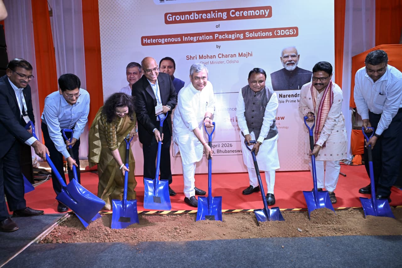
High-level presence underlines strategic importance
The foundation stone of the Heterogeneous Integration Packaging Solutions project, promoted by 3D Glass Solutions, was laid in the presence of Chief Minister Mohan Charan Majhi and Union Minister for Railways, Electronics & Information Technology, and Information & Broadcasting Ashwini Vaishnaw. With the launch of this project, Odisha is poised to become home to one of the world’s most sophisticated chip packaging technologies.
Global interest signals growing industrial strength
Global technology leaders such as Intel, Lockheed Martin, and Applied Materials are associated with cutting-edge packaging technologies, and their interest in Odisha reflects the state’s growing industrial strength.
The products manufactured in the state will support next-generation sectors such as Artificial Intelligence, high-performance computing, defence electronics, telecommunications, and advanced digital systems.
Investment, capacity and strategic edge
The company is investing nearly ₹2,000 crore in the project, and the facility is expected to produce 70,000 glass panels annually, along with 50 million assembled units and around 13,000 advanced 3DHI modules. He added that Odisha has emerged as the only state in the country where both India’s first compound semiconductor fabrication unit and the first 3D glass substrate packaging facility are being established.
Vaishnaw said that Odisha, traditionally known for its strengths in minerals, metals, and energy, is now steadily establishing itself in advanced sectors such as electronics, IT, and semiconductors. Describing the project as one of the most advanced manufacturing initiatives of its kind, he said it would significantly strengthen India’s semiconductor value chain.
Execution model and policy backing
The project is being implemented by 3D Glass Solutions Inc. (3DGS), USA, through its wholly owned Indian subsidiary Heterogeneous Integration Packaging Solutions Pvt. Ltd. (HIPSPL) at Info Valley in Khordha district. It is a greenfield, vertically integrated advanced packaging and embedded glass substrate ATMP facility.
The total investment in the project is ₹1,943.53 crore, including approved Central fiscal support of ₹799 crore and additional State support of approximately ₹399.5 crore.
Target markets and production timeline
The facility will cater to high-growth sectors such as data centres, Artificial Intelligence, machine learning, 5G/6G communications, automotive radar, defence electronics, aerospace applications, and photonics. Commercial production is expected to begin by August 2028, while full-scale volume production is targeted by August 2030.